
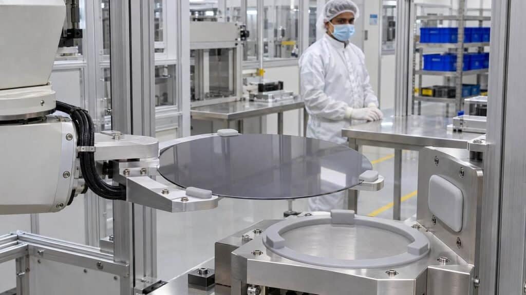
Silicone Moulding helps semiconductor equipment makers produce compliant contact pads, vacuum-handling parts, sealing elements, locating components, and protective interfaces for wafer-handling systems. When the compound and molded geometry are selected carefully, these components can support controlled wafer movement while helping reduce unnecessary contact stress, slipping, and damage to sensitive equipment surfaces.
Wafer handling is a small part of a semiconductor process, yet it carries real risk. A wafer can be thin, fragile, and highly sensitive to particles, static charge, and contact marks. The rubber component used in a robot end effector, vacuum pick-up tool, inspection station, or handling fixture must therefore match the process environment instead of being treated as a standard soft part.
Why wafer-handling components need precision
A wafer-handling component has to do more than make contact. It must hold or support the wafer consistently without causing excessive local pressure. The contact surface, hardness, shape, and surface finish can all affect how the wafer behaves during pick-up, movement, placement, and release.
Custom Rubber Moulding Products & Parts can be developed around the actual contact point and tool design. This allows the silicone part to suit the holder, mounting arrangement, wafer size, required movement, and available space within the machine.
A part that is too firm can create unwanted pressure at the contact point. A part that is too soft may deform excessively or allow the wafer to shift. The right design needs a balance between grip, support, controlled release, and long-term shape retention.
Where silicone molded components are used
Silicone molded parts can be used at several points within semiconductor manufacturing and wafer-handling equipment:
- Vacuum cups and compliant pick-up pads
- End-effector contact surfaces on wafer-transfer robots
- Protective locating pads and support points
- Seals around equipment covers, doors, and access areas
- Cushioning components in inspection or transfer fixtures
- Protective interfaces between delicate components and hard metal tooling
The application determines whether the component touches the wafer directly, supports a fixture, or seals a controlled equipment area. A direct-contact part needs particular attention to surface finish, cleanliness, and particle control. A seal or cushioning part may have different mechanical and environmental requirements.
A realistic wafer-transfer example
Consider a wafer-transfer station that moves wafers between a cassette, inspection tool, and process chamber. The robot end effector uses small molded silicone contact pads or vacuum-handling elements to lift and place the wafer.
The component must hold the wafer securely during acceleration and deceleration while avoiding marks, edge damage, or unstable contact. If the molded contact area is uneven, has rough flash, or collects contamination during use, it can create problems at the point where the tool meets the wafer.
This is why precision moulding matters. The shape must be repeatable, the surface must be suitable for the intended contact, and the part must fit the end effector correctly. A slight change in thickness or geometry can affect the tool’s alignment and handling consistency.
Cleanliness is part of the design
In semiconductor production, a component can perform mechanically and still be unsuitable for the application if it becomes a source of particles or unwanted emissions. Silicone Moulding for cleanroom or wafer-handling use should take account of the compound formulation, mould condition, surface finish, post-mould cleaning, handling, and packaging.
The part should also be assessed according to where it will be installed. A molded pad inside a wafer-handling path may need a different cleanliness standard from a component fitted outside the controlled process area. The equipment manufacturer should define the required particle, outgassing, and cleaning expectations before the component is finalised.
ESD, temperature, and chemical exposure need separate attention
Standard silicone is not automatically antistatic or conductive. If the equipment needs controlled electrostatic discharge or electrical continuity, the component may require a conductive or antistatic formulation. The required electrical properties should be defined by the equipment application, rather than assumed from the silicone material alone.
For semiconductor equipment where sealing and electrostatic control must work together, see Conductive Elastomers for EMI Shielding and Electrostatic Control in Semiconductor Manufacturing.
Temperature and chemical exposure should also be checked early. Some molded silicone components may operate near heated tools or controlled environments, while others may be exposed to cleaning processes, vacuum conditions, or nearby chemicals. The material choice must match those conditions. A part suited for a dry handling station may not be suitable for a location with aggressive chemical exposure.
Details that help develop a custom molded component
A useful enquiry should include the part drawing, mounting arrangement, required dimensions, hardness preference, contact geometry, operating temperature, and expected cycle frequency. For wafer-contact applications, it also helps to specify whether the component touches the wafer face, edge, backside, or a tool interface.
Information about static-control requirements, cleaning procedures, cleanroom handling, and any nearby process chemicals gives the supplier a clearer basis for selecting the compound and moulding approach.
Precision silicone components support the controlled movement and protection of sensitive semiconductor equipment. To explore customised rubber solutions for specialised manufacturing applications, visit Shree Rubber Works.
The best component design begins with the real tool conditions, not a generic part shape. Share the equipment drawing and application details before finalising the material or geometry. For support with a custom requirement, contact our team.